
<think>**Translating headline to English** </think> Samsung Bets on Homegrown Large Models, Enters Chip Manufacturing
<think>**Clarifying translation requirements and content** </think> On September 9, Samsung Electronics and France-based Mistral AI signed a strategic partnership agreement to combine semiconductor technology, manufacturing data, and efficient model capabilities to develop specialized AI models for design and manufacturing processes and deploy them in Samsung’s internal data centers.
<think>Planning faithful markdown translation
</think>Samsung Bets on Local Large Models, Expanding into Chip Manufacturing
Samsung Electronics is moving generative AI beyond office assistants and knowledge bases into the core workflows of chip design, wafer manufacturing, and yield management.
On September 9, Samsung Electronics confirmed that it had signed a strategic cooperation agreement with French artificial intelligence company Mistral AI. The two sides will leverage the semiconductor technologies and manufacturing data of Samsung Electronics’ Device Solutions (DS) division, together with Mistral AI’s model technology, to jointly develop a specialized AI model for semiconductor design and manufacturing.
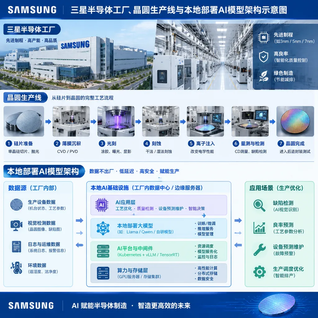
This is not a simple model procurement deal. Samsung plans to deploy the model locally on its internal infrastructure, then gradually integrate it into production processes such as data analysis, defect prediction, and process optimization. In other words, Samsung is not trying to build a “chatbot that understands chips,” but rather an industrial AI system capable of entering the factory data loop and participating in engineering decisions.
Keeping the Model On-Premises Is First and Foremost a Security Issue
Semiconductor companies are willing to embrace AI, but they are unlikely to hand their most critical production data directly to the public cloud.
The data generated by wafer fabs goes far beyond equipment logs. It includes process parameters, machine status, wafer inspection results, defect images, yield fluctuations, material batches, recipe adjustment records, and years of accumulated engineering experience across different process nodes. If this data were leaked, it could reveal a company’s process capabilities, equipment tuning methods, and product road maps.
That is why Samsung has placed particular emphasis on “local deployment” this time. Based on publicly available information, the relevant models will run on Samsung’s own servers, data centers, or within its production networks, rather than relying by default on external APIs. For Samsung, this deployment model offers at least three benefits:
- Data remains within the internal environment: Manufacturing data, customer information, and process recipes can remain within Samsung’s security perimeter.
- Easier integration with production systems: The model can establish connections with MES, FDC, SPC, quality management systems, and equipment log platforms.
- More controllable latency and stability: In a factory environment, defect alerts and equipment anomaly analysis cannot depend entirely on public-network connectivity or third-party cloud services.
This is also where Mistral AI may have an advantage over many purely cloud-based model providers when it comes to entering companies’ core workflows. Mistral AI was founded by researchers from organizations including Google DeepMind and Meta, and has long emphasized high-performance models, deployment flexibility, and data security. Its product roadmap is not limited to consumer-oriented chat applications; it also includes solutions for running models on companies’ own infrastructure.
However, local deployment does not mean that “installing the model” is enough to put it into production. Samsung will still need to address a range of engineering issues, including GPU resource scheduling, inference latency, model quantization, access isolation, data de-identification, audit trails, and model updates. In particular, in a wafer-fab environment, AI systems generally cannot directly replace process engineers in making irreversible adjustments. A more realistic approach is to first provide recommendations and rank risks, with engineers confirming execution.
For Semiconductor-Specific Models, the Challenge Is Not Chat Capability
If one looks only at the text-based question-answering capabilities of large language models, Samsung could simply call a general-purpose model. But the capabilities required for chip design and manufacturing are not the same as those needed to write emails or summarize documents.
During the design phase, a model may need to understand specifications, process design rules, verification reports, layout-check results, and historical project documents. During manufacturing, it must process structured sensor data, time-series data, defect images, and engineers’ natural-language records at the same time. There are also strong causal relationships among these different types of data: a change in temperature may not immediately cause a defect, but could manifest as a yield decline several batches later.
Therefore, the real technical challenges of this cooperation include:
- Multimodal data integration: Bringing text, tables, time-series signals, images, and equipment logs into a unified analytical framework.
- Industry knowledge injection: Enabling the model to understand process steps, equipment parameters, material properties, and manufacturing constraints, rather than generating answers solely based on statistical patterns in language.
- Causal and time-series analysis: Distinguishing correlation from causation and determining whether yield fluctuations originate from equipment, materials, recipes, or environmental changes.
- Explainable results: In high-value manufacturing scenarios, engineers need to know why the model issued a particular alert and which batches and parameters it relied on.
- Stability and reproducibility: The same set of process data should, under the same version and configuration, produce consistent and auditable analytical results as much as possible.
In terms of implementation sequence, Samsung is more likely to first use the model for knowledge retrieval, engineering report analysis, and anomaly attribution, before gradually advancing to defect prediction, process-window recommendations, and equipment maintenance. The former tasks carry lower risks and are easier to validate using historical data. The latter directly affect production-line throughput and yield and therefore require long-term pilot testing.
What Samsung Wants Most Is Yield, Not a Better Chat Experience
Public information indicates that Samsung plans to gradually apply the technology to data analysis, defect prediction, and process optimization in semiconductor business design and manufacturing operations, with the aim of shortening development times and improving manufacturing efficiency and product quality. Supplementary reports have also noted that Samsung hopes to use targeted AI models to improve manufacturing precision for advanced memory chips and stabilize yields.
These application areas are the true commercial core of the cooperation.
For manufacturers of memory and logic chips, even a small increase in yield can directly affect profits. Advanced processes require enormous equipment investments and involve complex production flows. If a defect pattern is not identified in time, the loss may involve not just a few wafers, but the scrapping of an entire batch, occupied capacity, and delayed deliveries.
The value of AI in this context lies primarily not in replacing engineers, but in connecting information that was previously scattered across different systems, shifts, and teams. For example, when a certain type of defect appears at multiple factories, the model can quickly retrieve historical cases, compare equipment status, material batches, and process parameters, and provide a ranked list of possible causes. When small changes occur in the vibration, temperature, or pressure signals of a piece of equipment, the model can combine them with past failure records to provide early warnings about maintenance windows.
These scenarios are closer to an “industrial decision-making system” than to a traditional Copilot. Whether the model’s output is useful will ultimately depend on whether it can reduce the time engineers spend troubleshooting, lower the number of trial-and-error attempts, and improve first-pass yield—not on whether it can write a fluent piece of natural language.
Why Mistral AI Was Able to Enter Samsung’s Core Business
From the perspective of supplier selection, Samsung did not limit this cooperation to the traditional cloud-provider ecosystem. Mistral AI’s characteristics may have been an important factor.
Mistral AI’s model strategy emphasizes efficiency and deployment flexibility. For Samsung, which operates large-scale data centers and complex production networks, a model that can be deployed, fine-tuned, and customized according to its internal computing resources is better suited to core manufacturing processes than a black-box system accessible only through an external cloud API.
At the same time, Samsung is also an important investor in Mistral AI’s recent financing. According to public reports, Mistral AI raised approximately €3 billion through a new funding round led by Samsung. Samsung Electronics was one of the lead investors, while institutions including EQT-managed European funds and PSG Equity also participated. The capital relationship means the cooperation is not merely a procurement relationship; it also provides a foundation for long-term joint product development and commercialization.
However, this does not mean that Mistral AI has already established a definitive advantage in semiconductor AI. It still needs to prove three things: how accurate its models are on real-world process data; whether they can adapt to Samsung’s existing software and equipment systems; and whether maintenance costs will remain manageable after large-scale deployment across factories.
Competition in semiconductor AI will ultimately not be determined solely by model parameter counts. The company that can truly connect models, data governance, edge computing, factory software, and engineering processes is more likely to build a durable competitive barrier.
This Is Not Samsung’s First Bet on an “AI Factory”
Samsung has already been advancing the construction of larger-scale AI infrastructure. NVIDIA previously disclosed that the two companies planned to build an AI factory for Samsung’s semiconductor manufacturing operations based on more than 50,000 NVIDIA GPUs, for applications including predictive maintenance, process improvements, and autonomous factories.
Mistral AI’s role in this cooperation does not completely conflict with NVIDIA’s. NVIDIA is more focused on providing computing infrastructure, accelerated platforms, and digital-twin tools, while Mistral AI provides model capabilities and enterprise AI software solutions. The former answers the question of “where the computing power is,” while the latter addresses “how the model understands corporate data and participates in the business.”
This also suggests that Samsung’s strategy may not be to bet on a single model provider, but to build a layered AI-factory system: GPUs, networks, and storage at the bottom; data platforms and production systems in the middle; and specialized models for design, manufacturing, quality, and supply chains at the top.
For Samsung, this combination also has practical significance. As advanced chip manufacturing becomes increasingly complex, it is difficult to improve efficiency linearly simply by adding equipment or expanding engineering teams. AI can turn experience previously dependent on a small number of senior engineers into system capabilities that can be searched, analyzed, and reused. However, whether digitized experience can truly translate into improved yield and capacity still needs to be validated with on-site data.
Samsung Hopes to Move from Point Applications to an Ecosystem Platform
Samsung said it will expand the cooperation in the future to businesses including memory chips, foundry, and logic chips within the DS division. It will also continue seeking AI application scenarios optimized for the semiconductor industry and further connect customers and partners.
This suggests that Samsung’s goal may extend beyond improving internal efficiency. If the model and platform are successfully validated in its own factories, Samsung may eventually be able to extend some of these capabilities to equipment suppliers, materials manufacturers, foundry customers, and design partners, creating an AI ecosystem around the semiconductor supply chain.
However, this step will be significantly more difficult than internal deployment. Data permissions, equipment protocols, process nodes, and quality standards vary among customers. Cross-company data sharing also involves trade secrets and the allocation of responsibility. If Samsung wants to turn its internal model into an ecosystem platform, it must establish clear mechanisms for data isolation, access control, and model accountability.
At present, the two sides have not disclosed the specific name of the specialized model, its parameter scale, the volume of training data, launch timeline, or quantified performance targets. Therefore, at this stage, it is more appropriate to view the cooperation as a clearly defined strategic initiative rather than a product launch that has already completed commercial validation.
Assessment: For Semiconductor Large Models, the Competition Is About Closed-Loop Capabilities
The cooperation between Samsung and Mistral AI is worth watching, but it should not be simply interpreted as “a European model provider has won Samsung.” What truly matters is that global chip manufacturers are moving the AI competition beyond office software and customer-service systems into process technology, equipment, and yield—the most difficult and most valuable areas.
Mistral AI’s advantages lie in model efficiency, deployment flexibility, and its security positioning in the European enterprise market. Samsung’s advantages include its global manufacturing network, vast amounts of factory data, and business scenarios spanning memory, foundry, and logic chips. Whether the two sides succeed will depend on whether these two sets of capabilities can genuinely be combined, not on how much attention the cooperation agreement attracts.
For developers, this case also sends a clear signal: the next stage of enterprise AI will not simply involve connecting general-purpose large models to knowledge bases. Instead, it will rebuild data, models, and business processes around specific industries. General-purpose models will handle understanding and reasoning, industry data will define the boundaries, production systems will carry out execution, and engineers will supervise and correct the process.
If Samsung can ultimately turn defect prediction, process optimization, and engineering knowledge management into a reusable platform, it will gain more than just a model—it will gain a new manufacturing operating system. Conversely, if the model remains limited to report summarization and question answering, the value of this cooperation will be greatly diminished.
As of September 9, 2026, Samsung’s direction is already clear: the model is to be deployed locally, data is to enter a closed loop, and applications are to penetrate the design and manufacturing floors. What truly deserves attention next is not the model’s parameter count at a launch event, but whether Samsung’s yield, development cycle, and factory efficiency show verifiable improvement.
References
- ITHome: Samsung Electronics and Mistral AI Reach Strategic Cooperation to Jointly Build a Semiconductor-Specific Artificial Intelligence Model — Provides core information on the agreement between the two sides, local deployment, and application areas.
- ITHome: Reports Related to Samsung’s Cooperation with Mistral AI — Used to cross-check the industry background of the cooperation between Samsung and Mistral AI.