
Intel Bets on Musk’s Terafab: Can the IDM Model Reshape Chip Manufacturing?

Intel has officially joined Musk’s Terafab project, aiming for an annual production capacity of 1 TW of computing power. This marks a key breakthrough for Intel’s foundry business and represents a direct challenge from Musk to TSMC’s dominant foundry model.
Intel Bets on Musk’s Terafab: Can the IDM Model Reshape Chip Manufacturing?
Intel today announced its participation in Elon Musk’s Terafab initiative, joining forces with Tesla, SpaceX, and xAI to build a new generation of chip manufacturing system. The project aims to produce 1 terawatt (TW) of computing power per year—far exceeding the scale of any current single semiconductor fab.
This is not a simple collaboration. Intel CEO Pat Gelsinger’s statement revealed deeper intentions: “Terafab represents a fundamental transformation in how silicon logic, memory, and packaging are manufactured.” In plain terms, Musk wants to use the IDM (Integrated Device Manufacturer) model to challenge TSMC’s foundry-dominated production system, and Intel happens to need a major client to support its foundry business.
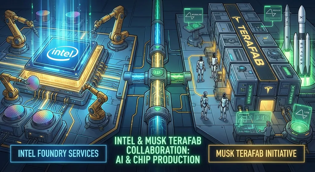
The Return of the IDM Model: Old Path or New Approach
Terafab’s IDM model essentially means designing, manufacturing, and packaging chips in-house. This was Intel’s winning approach in the PC era, but over the past decade, it was beaten down by TSMC’s specialized foundry model. So why is Musk bringing it back now?
The key is the efficiency of vertical integration. Tesla’s car production and SpaceX’s rocket manufacturing both follow this philosophy—control critical supply chain stages and iterate quickly. xAI’s Grok model training capacity doubles on a monthly basis; if it relied on external foundries with production queues, it would never keep up. Terafab’s logic is: design the chips yourself, build them yourself, and fix problems directly on the production line—no waiting for another fabrication cycle.
But there’s a prerequisite—having enough internal demand to justify the capacity. Intel’s IDM collapse happened because its own CPU demand couldn’t sustain enormous investments in advanced nodes, while TSMC shared costs across global clients. Musk’s advantage is that Tesla’s FSD chips, xAI’s training chips, and Starlink’s satellite chips add up to a genuinely massive volume.
What 1TW of Computing Power Means
Terafab’s goal is an annual output of 1TW of computing power. How big is that?
The world’s largest AI training clusters, like Meta’s Grand Teton, have around 100–200 petawatts (PW). 1TW = 1000PW, equivalent to the yearly capacity of 5–10 Grand Teton clusters. Based on the performance density of Nvidia’s H100 GPUs, that translates to roughly 2–3 million high-performance AI chips annually.
This isn’t just “building a few data centers”—it means creating a fully independent semiconductor ecosystem. Musk said at Tesla’s 2025 shareholder meeting that Terafab would be “much larger” than Tesla’s Gigafactories. Considering Tesla’s Shanghai factory covers 2 million square meters, Terafab could exceed 5 million square meters—nearly the total area of all TSMC fabs combined.
What Intel Gains
For Intel, this is a lifeline for its foundry business (IFS).
Since launching its IDM 2.0 strategy in 2021, Intel has tried to open its manufacturing capability to external clients. But after three years, beyond small trial orders from Qualcomm and Amazon, no major client has come onboard. The reason: why would customers trust a foundry that struggled with 10nm for five years?
Terafab gives Intel a chance to prove itself. Musk’s project tolerates lower yield rates—AI training chips can handle defective cores by disabling them through software. This lets Intel iterate quickly on its 18A process. If Intel can make 18A work for Terafab, it can use that case to convince other clients.
Packaging technology is even more crucial. Intel’s Foveros and EMIB 3D packaging technologies truly shine in high-performance computing settings. xAI’s Colossus cluster interconnects 100,000 H100s, posing major power and heat challenges. If 3D packaging can stack compute chips, HBM memory, and network chips together, it would significantly reduce power consumption and latency—something TSMC’s CoWoS packaging can’t easily achieve.
Can This Actually Work?
Frankly, it’s full of uncertainties.
The biggest problem with IDM is capital efficiency. A single TSMC 5nm fab costs $20 billion to build but serves dozens of clients—Apple, Nvidia, AMD—so each only bears a small portion. If Terafab builds its own lines, Musk must shoulder the entire $20 billion himself. Even if Tesla, SpaceX, and xAI have the cash flow, the opportunity cost is astronomical.
Then there’s talent and supply chain complexity. TSMC spent 30 years building its engineering teams and supplier network—it can’t be copied with money alone. Intel’s 10nm struggles are proof: buying ASML’s EUV machines is easy, mastering them takes thousands of engineers years of tuning. Terafab’s plan to build production lines within 2–3 years is exceedingly hard.
Yet Musk has one advantage—he doesn’t need cutting-edge nodes. Tesla’s FSD chips use 14nm, Starlink’s satellite chips run on 28nm—these mature processes and tools are ready to go. If Terafab focuses on the 7–14nm range, stacking computing power through mature nodes, technical risk drops significantly. xAI’s training chips could adopt chiplet architectures, packaging multiple 7nm dies together—the performance may rival TSMC’s 3nm chips.
Industry Impact
If Terafab actually takes off, its most direct impact would be on TSMC’s pricing power.
Currently, TSMC monopolizes the AI chip market—Nvidia, AMD, and Google’s TPUs are all fabbed there. With no Plan B, clients accept its pricing and schedules. If Terafab can provide 1TW of annual output, that’s a 20–30% increase in global supply, cutting into TSMC’s premium margins.
The deeper impact is on the foundry model itself. For 20 years, the semiconductor consensus has been “specialized division of labor yields maximum efficiency”—design houses design, foundries manufacture. But the AI era’s demand evolves too fast; design and manufacturing need tight coupling. If Terafab proves IDM is more efficient for AI chips, it could spark a wave of vertical integration.
For developers, the significance is in computation costs. Training a large model today can cost tens of millions of dollars, mostly due to chip costs. If Terafab scales AI chip supply by an order of magnitude, computational costs could drop to one-third—or even one-fifth—of current levels. That would reshape AI’s economic model: many use cases unfeasible today due to compute costs might become viable within a few years.
Intel’s Big Gamble
When Gelsinger said “Intel is honored to be a partner,” it sounded polite—but in reality, Intel is betting the future of its foundry business on Musk.
If Terafab succeeds, Intel’s 18A process could revive, and IFS would secure sustained large-scale orders. If it fails, Intel’s investments in advanced nodes would be wasted, and its foundry business could flatline.
But Intel doesn’t have many choices. In AI chips, Intel has fallen far behind Nvidia. Its CPU business is being eroded by AMD and ARM; discrete graphics (Arc series) gained little traction. Foundry is the only battlefield where Intel still has a shot—and Terafab is now its biggest visible opportunity.
Musk’s philosophy is “be number one or die trying.” SpaceX nearly went bankrupt three times before succeeding; Tesla spent two years in the Model 3 production hell. Terafab will likely follow a similar path—early chaos and skepticism, then exponential growth once it clicks.
Intel’s job now is to make sure its 18A process and packaging tech are operational before Musk “dies on the road.” The window may only last 18–24 months.
Final Thoughts
Terafab, at its core, is a high-stakes gamble: betting that AI compute demand will keep exploding, that vertical integration beats specialized division, and that Intel’s manufacturing muscle still matters.
If any of these bets fail, the whole project could collapse. But if they all succeed, the semiconductor landscape could undergo the biggest shift in 20 years.
For developers, the takeaway is clear: if Terafab truly drives compute costs down, many AI applications currently confined to labs could become commercially viable within 2–3 years. That window might arrive faster than most expect.
References
- Intel joins Terafab with Tesla, SpaceX, and xAI to transform chip manufacturing – IT Home
Official announcement from Intel about its participation in the Terafab project